- 您现在的位置:买卖IC网 > Sheet目录3890 > PIC16C717T-E/SS (Microchip Technology)IC MCU OTP 2KX14 A/D PWM 20SSOP
PIC16C717/770/771
DS41120B-page 106
2002 Microchip Technology Inc.
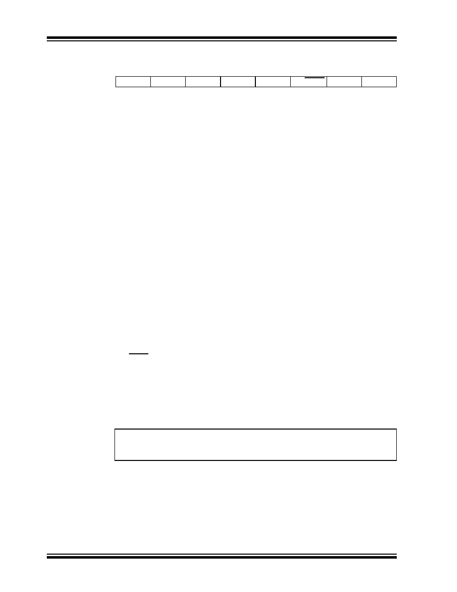
REGISTER 11-1:
A/D CONTROL REGISTER 0 (ADCON0: 1Fh).
R/W-0
ADCS1
ADCS0
CHS2
CHS1
CHS0
GO/DONE
CHS3
ADON
bit 7
bit 0
bit 7-6
ADCS<1:0>: A/D Conversion Clock Select bits
If internal VRL and/or VRH are not used for A/D reference (VCFG<2:0> = 000, 001, 011
or 101):
00
= FOSC/2
01
= FOSC/8
10
= FOSC/32
11
= FRC (clock derived from a dedicated RC oscillator)
If internal VRL and/or VRH are used for A/D reference (VCFG<2:0> = 010, 100, 110 or 111):
00
= FOSC/16
01
= FOSC/64
10
= FOSC/256
11
= FRC/8
bit 5-3,1
CHS:<3:0>: Analog Channel Select bits
0000
= channel 00 (AN0)
0001
= channel 01 (AN1)
0010
= channel 02 (AN2)
0011
= channel 03 (AN3)
0100
= channel 04 (AN4)
0101
= channel 05 (AN5)
0110
= reserved, do not select
0111
= reserved, do not select
1000
= reserved, do not select
1001
= reserved, do not select
1010
= reserved, do not select
1011
= reserved, do not select
1100
= reserved, do not select
1101
= reserved, do not select
1110
= reserved, do not select
1111
= reserved, do not select
bit 2
GO/DONE: A/D Conversion Status bit
1
= A/D conversion cycle in progress. Setting this bit starts an A/D conversion cycle.
This bit is automatically cleared by hardware when the A/D conversion has completed.
0
= A/D conversion completed/not in progress
bit 0
ADON: A/D On bit
1
= A/D converter module is operating
0
= A/D converter is shutoff and consumes no operating current
Legend:
R = Readable bit
W = Writable bit
U = Unimplemented bit, read as ‘0’
- n = Value at POR
’1’ = Bit is set
’0’ = Bit is cleared
x = Bit is unknown
发布紧急采购,3分钟左右您将得到回复。
相关PDF资料
PIC16LC770T-E/SO
IC MCU OTP 2KX14 A/D PWM 20SOIC
PIC16C771T/SO
IC MCU OTP 4KX14 A/D PWM 20SOIC
PIC16LC717T-I/SS
IC MCU OTP 2KX14 A/D PWM 20SSOP
PIC16C717T/SS
IC MCU OTP 2KX14 A/D PWM 20SSOP
PIC16LC770T-I/SO
IC MCU OTP 2KX14 A/D PWM 20SOIC
PIC16LC771T-E/SS
IC MCU OTP 4KX14 A/D PWM 20SSOP
PIC16C771T-E/SS
IC MCU OTP 4KX14 A/D PWM 20SSOP
PIC16LC771T-I/SO
IC MCU OTP 4KX14 A/D PWM 20SOIC
相关代理商/技术参数
PIC16C717T-I/SO
功能描述:8位微控制器 -MCU 3.5KB 256 RAM 16 I/O RoHS:否 制造商:Silicon Labs 核心:8051 处理器系列:C8051F39x 数据总线宽度:8 bit 最大时钟频率:50 MHz 程序存储器大小:16 KB 数据 RAM 大小:1 KB 片上 ADC:Yes 工作电源电压:1.8 V to 3.6 V 工作温度范围:- 40 C to + 105 C 封装 / 箱体:QFN-20 安装风格:SMD/SMT
PIC16C717T-I/SS
功能描述:8位微控制器 -MCU 3.5KB 256 RAM 16 I/O RoHS:否 制造商:Silicon Labs 核心:8051 处理器系列:C8051F39x 数据总线宽度:8 bit 最大时钟频率:50 MHz 程序存储器大小:16 KB 数据 RAM 大小:1 KB 片上 ADC:Yes 工作电源电压:1.8 V to 3.6 V 工作温度范围:- 40 C to + 105 C 封装 / 箱体:QFN-20 安装风格:SMD/SMT
PIC16C71T-04/SO
功能描述:8位微控制器 -MCU 1.75KB 36 RAM 13 I/O 4MHz SOIC18 RoHS:否 制造商:Silicon Labs 核心:8051 处理器系列:C8051F39x 数据总线宽度:8 bit 最大时钟频率:50 MHz 程序存储器大小:16 KB 数据 RAM 大小:1 KB 片上 ADC:Yes 工作电源电压:1.8 V to 3.6 V 工作温度范围:- 40 C to + 105 C 封装 / 箱体:QFN-20 安装风格:SMD/SMT
PIC16C71T-04I/SO
功能描述:8位微控制器 -MCU 1.75KB 36 RAM 13 I/O 4MHz Ind Temp SOIC18 RoHS:否 制造商:Silicon Labs 核心:8051 处理器系列:C8051F39x 数据总线宽度:8 bit 最大时钟频率:50 MHz 程序存储器大小:16 KB 数据 RAM 大小:1 KB 片上 ADC:Yes 工作电源电压:1.8 V to 3.6 V 工作温度范围:- 40 C to + 105 C 封装 / 箱体:QFN-20 安装风格:SMD/SMT
PIC16C71T-20/SO
功能描述:8位微控制器 -MCU 1.75KB 36 RAM 13 I/O RoHS:否 制造商:Silicon Labs 核心:8051 处理器系列:C8051F39x 数据总线宽度:8 bit 最大时钟频率:50 MHz 程序存储器大小:16 KB 数据 RAM 大小:1 KB 片上 ADC:Yes 工作电源电压:1.8 V to 3.6 V 工作温度范围:- 40 C to + 105 C 封装 / 箱体:QFN-20 安装风格:SMD/SMT
PIC16C71T-20I/SO
功能描述:8位微控制器 -MCU 1.75KB 36 RAM 13 I/O RoHS:否 制造商:Silicon Labs 核心:8051 处理器系列:C8051F39x 数据总线宽度:8 bit 最大时钟频率:50 MHz 程序存储器大小:16 KB 数据 RAM 大小:1 KB 片上 ADC:Yes 工作电源电压:1.8 V to 3.6 V 工作温度范围:- 40 C to + 105 C 封装 / 箱体:QFN-20 安装风格:SMD/SMT
PIC16C72/JW
功能描述:8位微控制器 -MCU 3.5KB 128 RAM 22 I/O RoHS:否 制造商:Silicon Labs 核心:8051 处理器系列:C8051F39x 数据总线宽度:8 bit 最大时钟频率:50 MHz 程序存储器大小:16 KB 数据 RAM 大小:1 KB 片上 ADC:Yes 工作电源电压:1.8 V to 3.6 V 工作温度范围:- 40 C to + 105 C 封装 / 箱体:QFN-20 安装风格:SMD/SMT
PIC16C72-04/SO
功能描述:8位微控制器 -MCU 3.5KB 128 RAM 22 I/O RoHS:否 制造商:Silicon Labs 核心:8051 处理器系列:C8051F39x 数据总线宽度:8 bit 最大时钟频率:50 MHz 程序存储器大小:16 KB 数据 RAM 大小:1 KB 片上 ADC:Yes 工作电源电压:1.8 V to 3.6 V 工作温度范围:- 40 C to + 105 C 封装 / 箱体:QFN-20 安装风格:SMD/SMT